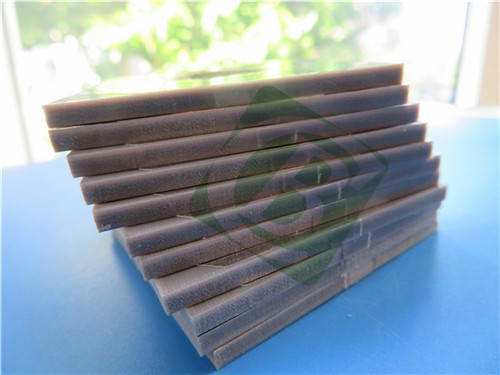
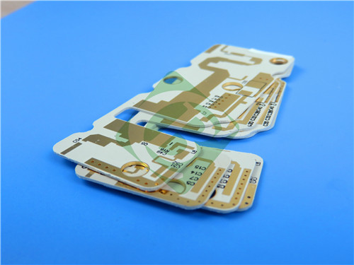
Double-Sided PCB with TP450, 2.6mm Thickness, ENIG Finish for High-Frequency Applications
(All PCBs are custom-manufactured. Reference images and parameters may vary based on your design requirements.)
1. Overview of the Double-Sided PCB
Our double-sided PCB is built with TP450, a unique thermoplastic material that combines ceramic fillers and polyphenylene oxide resin (PPO) for superior dielectric performance. With a 4.5 dielectric constant (Dk) and low dissipation factor (Df) of 0.0010 at 10 GHz, this PCB ensures signal integrity and minimal signal loss, even in demanding environments.
The ENIG surface finish enhances solderability and provides excellent corrosion resistance, while the 2-layer rigid design ensures structural stability. Although this PCB does not include solder masks or silkscreens, it is manufactured with 100% electrical testing to ensure performance and compliance with IPC-Class-2 standards.
2. PCB Construction Details
| Parameter | Specification |
| Base Material | TP450 |
| Layer Count | Double-sided |
| Board Dimensions | 121mm x 125mm ± 0.15mm |
| Minimum Trace/Space | 6/4 mils |
| Minimum Hole Size | 0.5mm |
| Via Type | No Blind Vias |
| Finished Board Thickness | 2.6mm |
| Finished Copper Weight | 1oz (1.4 mils) outer layers |
| Via Plating Thickness | 20 μm |
| Surface Finish | Electroless Nickel Immersion Gold (ENIG) |
| Top Solder Mask | None |
| Bottom Solder Mask | None |
| Top Silkscreen | None |
| Bottom Silkscreen | None |
| Electrical Testing | 100% tested to IPC-Class-2 standards |
3. PCB Stackup
The 2-layer rigid PCB stackup is straightforward yet effective for high-frequency designs. The stackup structure is as follows:
| Layer | Material | Thickness |
| Copper Layer 1 | Copper (1oz) | 35 μm |
| Core Material | TP450 | 2.54mm (100mil) |
| Copper Layer 2 | Copper (1oz) | 35 μm |
4. Features of TP450 Material
- Dielectric Constant (Dk): 4.5 ± 0.2 at 10 GHz, ensuring stable signal transmission.
- Dissipation Factor (Df): 0.0010 at 10 GHz for minimal signal loss.
- Thermal Stability: Low TCDk: -50 ppm/°C, ensuring stable dielectric performance over temperature changes.
- CTE: X-axis: 50 ppm/°C. Y-axis: 50 ppm/°C. Z-axis: 60 ppm/°C.
- Excellent reliability over a wide temperature range (-55°C to 150°C).
- Moisture Absorption: 0.01%, ensuring consistent performance in humid environments.
- Flammability Rating: UL 94 V-0 for enhanced safety.
- Thermal Conductivity: 0.44 W/mK, providing effective heat dissipation.
5. Benefits of TP450 Material
- Low Dielectric Loss: Ensures high signal integrity for RF and microwave applications.
- Thermal and Mechanical Reliability: With excellent CTE and thermal conductivity, it performs well in extreme environments, including space and defense applications.
- Stable Dielectric Constant: The Dk is tightly controlled and remains consistent across a wide temperature range, making it suitable for precision applications.
- Moisture Resistance: Low moisture absorption ensures consistent performance in humid or marine environments.
- Cost-Effective Manufacturing: The material is compatible with standard PCB processes, reducing production costs without compromising quality.
6. Applications of the Double-Sided PCB
Global Satellite Navigation Systems: Used in high-precision satellite communication and navigation devices.
Missile-Borne Applications: Ensures reliability in extreme environments with high vibration and thermal stress.
Miniaturized Antennas: Perfect for compact, high-performance RF antenna designs.
Fuze Technology: Ideal for sensitive and precision-guided systems.
The TP450-based double-sided PCB delivers excellent performance for critical RF and microwave systems, making it a reliable choice for advanced applications.
Why Choose Bicheng Technologies?
At Bicheng Technologies Limited, we specialize in designing and manufacturing high-quality PCBs for RF and microwave applications. Our double-sided PCB with TP450 material is manufactured to the highest standards, offering exceptional performance, reliability, and value.
Why Work With Us?
Global Reach: We deliver worldwide, ensuring timely support for your projects.
Quality Assurance: All PCBs are tested to IPC-Class-2 standards for guaranteed reliability.
Customer Support: We provide tailored solutions to meet your specific project requirements.
If you’re looking for a trusted partner for your next high-frequency project, feel free to contact Sally at sales30@bichengpcb.com. Let’s work together to bring your innovative designs to life.

|
|
TP450 Double-Sided PCB bulit on 2.5mm thick substrates with ENIG Finish for High-Frequency Applications Images
|